Institute for Communication Technologies and Embedded Systems

DAB

Digital Audio Broadcasting

Design of VLSI-Components for Digital Audio Broadcasting

Analog radio transmission services are in widespread use since the beginning of the century. Especially for mobile reception ("car radio'') the quality of the received audio programme suffers because of noise and signal drop-outs.

Therefore, during the years 1992-95 a digital transmission scheme for radio broadcasting has been defined which will resolve most of the problems inherient to the currently used analog transmission methods. This Digital Audio Broadcasting (DAB) scheme, as defined by the European Telecomunication Standard (ETS 300 401) will provide CD audio quality even for mobile receivers. DAB-based radio broadcasting will officially start in the year 1997 in Germany.

The poor quality of the mobile analog reception is caused by two effects. First, the received signal is disturbed by noise originating e.g. from other transmitters, electrical machines, car ignition, etc. Second, the transmitted signal interferes with itself because of multi-path signal propagation (due to reflections of the signal at buildings etc). Moreover, a moving receiver leads to changes of the interference and noise pattern over time ("fading'' multi-path effects).

These problems are solved by DAB by incorperating the following schemes (among others):
 

  • Forward Error-Correction (FEC) based on convolutional codes
  • Orthogonal Frequency Divison Multiplexing (OFDM) and
  • Redistribution of the data bits over some time interval (time interleaving)

The use of these methods will provide a high qualtity of service but it also leads to a very significant amount of digital signal processing at the receiver site. The mature digital CMOS VLSI technologies allow to implement DAB receivers in a cost-effective manor.

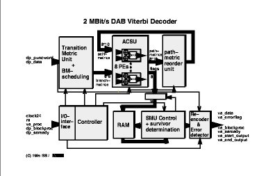
Our work - The first full-rate DAB Viterbi decoder

In a close co-operation with industry we are developing VLSI-components for the digital signal processing section of DAB receivers. During the last year we have developed a key component of the DAB receiver, the Viterbi Decoder. The Viterbi Decoder performs the error-correction of the received noise-disturbed signal.

Architecture of the DAB Viterbi Decoder

In this Viterbi Decoder at each data clock cycle 64 node equations have to be computed (each single computation requiring about 5 DSP instructions). The required data rate of 3 Mbit/s (``full-rate') therefore leads to 3*64*5 MOps/sec = 1 GOps/sec. Due to this high amount of equivalent DSP operations per second a standard programable DSP solution using an off-the-shelf DSP chip was impossible and a special ASIC (application specific integrated circuit) had to be developed.

Several VLSI architectures for Viterbi decoders are known from literature. But since the required data rate was higher than the data rate provided by node-serial architectures (they use a single processing element) and lower than that provided by traditional node-parallel architectures (N=64 Processing elements) a special architecture has been developed for an area-efficient solution. This architecture uses 8 processing elements. Using 8 processing elements to compute the 64 node equations saves silicon area but requires a somewhat complex scheduling scheme. The computation of the required schedules for this area-efficient class of Viterbi decoder architectures for medium speed may be found in the following paper:
"S. J. Bitterlich, H. Meyr, Efficient Scalable Architectures for Viterbi Decoders"
(published in Proceedings of the 1993 Conference on Application Specific Array Processors, Venice, Italy).

A comparision of the new Viterbi decoder architectures down to the VLSI layout level (for 1.0um CMOS semi-custom implementations) may be found in the paper:
"S. J. Bitterlich, H. Meyr, Area-Efficient Viterbi Decoder Macros"
(published in Proceedings of the 1994 European Solid-State Circuits Conference (ESSCIRC'94), Ulm, Germany).

Design Methodology

We used VHDL (Very High-level Hardware Description Language) to describe the VLSI-architecture. A state-of-the-art logic synthesis tool (Synopsys Design Compiler) has been used to synthesize a netlist for a CMOS composite gate array technology ( we also offer an VHDL-based ASIC-design course ; please refer to our lectures section [GERMAN])

Verification

The implementation has been verified by COSSAP-VHDL co-simulation: The system simulator COSSAP was used to generate a simulated noisy received signal and provided a perfect (floating-point) Viterbi Decoder (``golden device'') from its library. Simultaneously a VHDL simulator was used to execute the developed VHDL description of the DAB Viterbi Decoder. By (automatic) comparision of both results we verified the correctness of the developed VHDL code. In addition, our industry partners performed a gate-level simulation of the synthesized netlist to verify the synthesis process and the operating frequency of the design.

The details of the implemented ASIC and the design methodologies are presented in the paper (IN GERMAN): "S. J. Bitterlich, W. Brugger, G. Bergmann, H. Meyr, Ein Viterbi Decoder fuer den digitalen Rundfunk" (7. ITG Fachtagung Mikroelektronik fuer die Informationstechnik, Chemnitz, Germany, March 1996)

Future Work

We finished our work at the DAB Viterbi Decoder in Mid-1995. Currently we are implementing several other parts of the DAB receiver:

  • The frequency de-interleaver
  • A data block reformater / logical channel extractor
  • The time de-interleaver